
Controlled Dielectric or Controlled Impedance?
Confusion abounds regarding the topics of controlled dielectric and controlled impedance in the printed circuit board industry. We’ll try to clarify the subject.
Controlled Dielectric
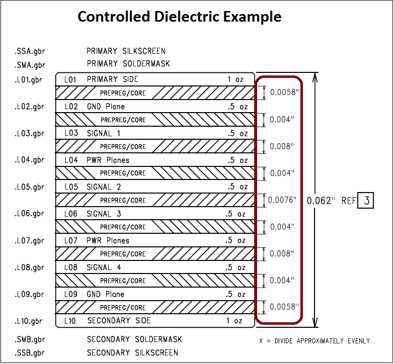
If you are an adventurous Electrical Engineer and you’d like to tackle the calculations yourself, you would be taking the Controlled Dielectric approach to control your own impedance. After making all the necessary calculations, you would need to specify in your fab exactly what dielectric spacing is needed between your copper layers as well as layout your traces with the correct trace and space. From a printed circuit board manufacturing perspective, all we would need to do is follow your design to meet your impedance. On our PCB Universe, Inc. Quote Form, you would need to select CONTROLLED DIELECTRIC since we would not be recalculating the impedance for you, nor testing the board to ensure the impedance is met. We would print the copper features on your board as we see them in the Gerber and use the dielectric stack that you specify.
Controlled Impedance
If you would rather have our engineers calculate the impedance for you, we would need to know which traces need to be controlled, what impedance is required and in reference to which copper layers. Select CONTROLLED IMPEDANCE on the Quote Form.
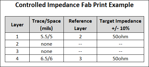
When ordering a board with Controlled Impedance from PCB Universe, Inc., we take the math out of the equation. We will calculate and correct your trace and space, use the correct dielectric spacing between your layers, and run a TDR test to confirm the correct impedance is met.
If you have any questions, please contact us. The definitions for these topics are below.
Dielectric can also mean an electrical insulator that can be polarized by an applied electric field. When a dielectric is placed in an electric field, electric charges do not flow through the material, as in a conductor, but only slightly shift from their average equilibrium positions causing dielectric polarization. Because of dielectric polarization, positive charges are displaced toward the field and negative charges shift in the opposite direction. This creates an internal electric field, which reduces the overall field within the dielectric itself.
To a PCB manufacturer, a controlled dielectric implies that specific thicknesses between layers are required.