
Via Tenting, Plugging, and Filling
There are many reasons a printed circuit board designer might want to have a via tented, plugged or filled. First, let's start with defining these terms since they can be frequently misused and misunderstood.
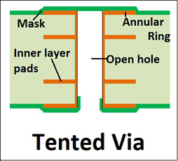
Via Tenting
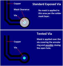 This is the easiest and least costly process—actually there is no added cost for this process. Simply remove the mask clearances from the vias you wish to have tented. Tenting a via simply means to cover the annular ring and via hole with solder mask. No special steps are taken to ensure the hole opening remains closed. Tenting a via will sometimes result in the hole remaining covered but it isn't guaranteed. Smaller diameter vias (12mil diameter or less) have the best chance of remaining closed. The main purpose for tenting shouldn't be to close the opening of a hole but rather, cover the annular ring to prevent exposure to the elements and reduce accidental shorting or contact with the circuit.
Mask (LPI) Plugged Vias (Non-Conductive Fill)
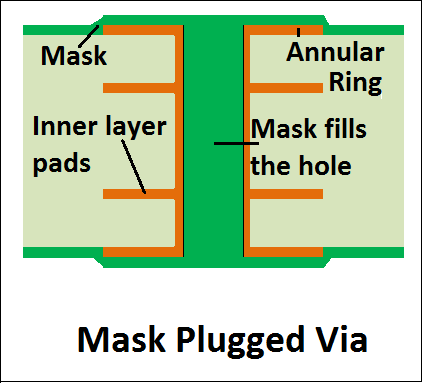
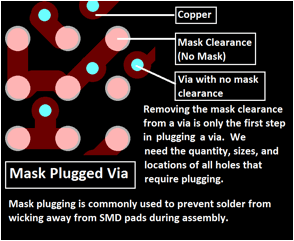 With a mask plugged via, (a.k.a. Mask Filled or Non-Conductive Filled via), specific measures are taken to ensure the via is plugged and sealed with mask and the annular ring is covered. A common application for this is on a BGA design where vias are commonly found in very close proximity to the BGA’s SMD pads. The concern is during assembly, solder will wick away from the intended pad and flow down the via creating poor or non-existent solder joints.
Via In Pad (Active Pad)
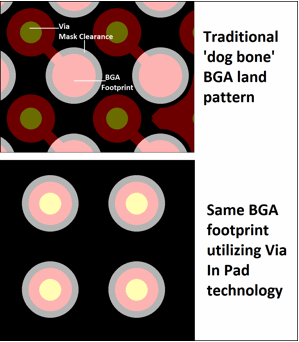 This process is becoming more and more common as BGA packages are becoming tighter. Rather than using the standard “dog bone” land pattern to transfer signal from the BGA footprint to a via that passes signal to other layers, vias can be drilled directly into the BGA footprint pads. This allows much simpler routing by soldering directly over the via. Make sure this process is called out in your fab notes.
- Drill the via (thru hole or blind)
- Fill the via with non-conductive material. Conductive material can be used but it’s not recommended since conductive material expands much more quickly than the surrounding laminate when heated which can cause cracks and pad failures during the assembly process.
- The surface of the plugged via is then plated over with copper.
- The newly plated copper surface is flattened and smoothed (planarized) to be even with the surrounding copper features.
- The final finish is applied
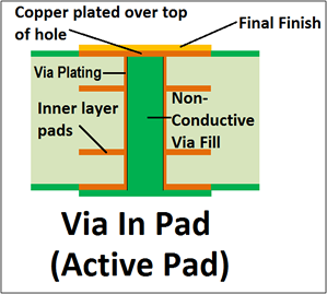 You now have a solderable surface mount pad that also passes signal to inner layers eliminating the need to rout the signal to a via on the surface layer.
Conductive vs Non-Conductive Filled Vias
The main drawback to conductive filled vias is the difference in CTE (Coefficient of Thermal Expansion) between the metallic fill and surrounding laminate. Metal will heat and expand much more rapidly than the surrounding laminate and this may cause fractures between the pads and hole wall. Because of this, conductive filled vias are not recommended for Via In Pad processing where the purpose of the fill is the reinforce the stability of the copper pad that is plated over the hole.
Vias Plated Shut with Copper
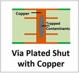 This is an older callout sometimes seen on legacy products. The original idea was to call for this as a way to have a copper conductive filled via. The problem with this process is that the holes must be extremely small to make this feasible since the copper used to to plate a via closed will also plate on all copper features on the board. (All vias and surface copper). Since 1oz of copper = 1.4mils, the amount of plating required to plate closed an 8 mil drilled hole is 2.8oz. 8mil/2 = 4 since plating is applied to both “sides” of the hole barrel. 4mil/1.4 = 2.85oz. This is 2.85oz additional copper to what is already on the surface of the board. This would bring the design’s total copper weight to 3.5 to 4oz. Tight space and trace designs are not possible with this amount of copper.
Another drawback is the extreme difficulty in plating the entire barrel of the hole evenly. A hole barrel will tend to plate faster toward the top and bottom of the hole which means a hole may look sealed but in the center there is trapped air and/or fluids which will outgas when exposed to assembly temperatures. We will not attempt this type of fill since far more reliable alternatives exist.